Designing electronics can feel complex at first—but the latest generation of KiCad makes the process far more approachable, while still offering the depth professionals expect. Whether you’re sketching a simple circuit or building a multi-layer board for a sophisticated product, KiCad provides a complete, integrated environment that guides you from idea to finished design.
What makes KiCad stand out is its balance: it’s powerful without being overwhelming, flexible without being confusing, and free without compromising capability. Below is a clear and vivid look at its key components and what makes them unique.
Schematic Capture: Turning Ideas into Clear Circuit Designs
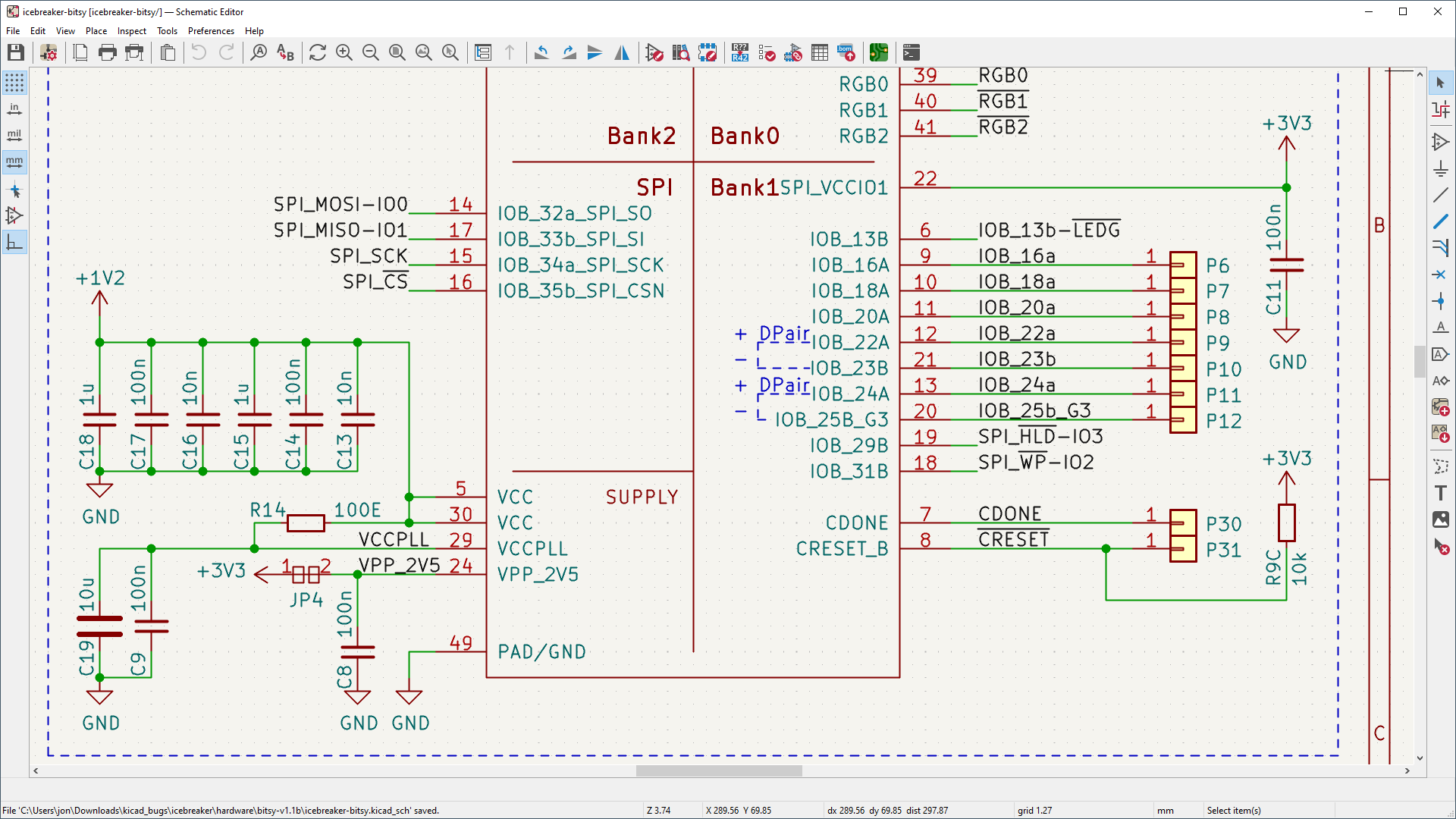
At the heart of any electronics project is the schematic—the blueprint that defines how components connect. KiCad’s schematic editor is designed to feel intuitive from the first click, yet it scales effortlessly as your project grows.
What makes it powerful?
- From simple to complex, seamlessly
You can start with a single-page circuit and expand into a hierarchical design with many interconnected sheets. This is especially useful when working on large systems, such as embedded controllers or communication devices. - Massive symbol libraries
KiCad includes thousands of ready-to-use component symbols. Need something custom? You can easily create your own symbols and reuse them across projects. - Clear organization with hierarchy
Imagine designing a device with separate power, control, and sensor sections. Instead of crowding everything onto one page, you can divide your design into logical blocks. Each block becomes easier to read, debug, and maintain. - Built-in simulation (SPICE)
Before building anything physically, you can simulate how your circuit behaves. For example, you can test how a voltage regulator responds to load changes or verify that an amplifier produces the expected output. - Electrical Rules Checker (ERC)
KiCad automatically scans your design for common mistakes—like unconnected pins or conflicting signals—helping you catch problems early.
👉 Example:
If you’re designing a microcontroller board, you can simulate the power supply section first, confirm stable voltage output, and then integrate it into the full schematic with confidence.
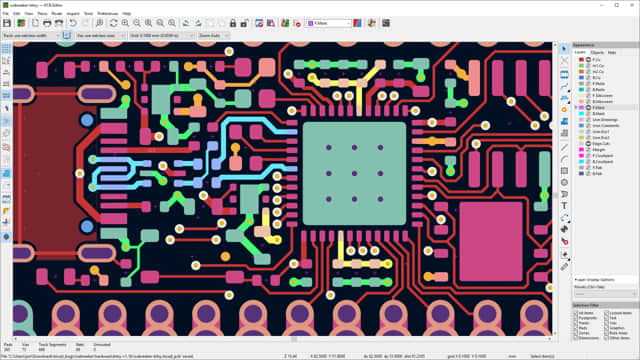
PCB Layout: From Concept to Physical Board
Why it stands out:
- Beginner-friendly, yet professional-grade
The interface makes it easy to place components and draw connections, even if it’s your first PCB. At the same time, it supports advanced features like multi-layer boards and high-speed design constraints. - Interactive router
Routing traces (the copper connections on a board) can be one of the most challenging steps. KiCad’s router actively helps you:- Avoid collisions
- Maintain spacing rules
- Automatically adjust paths for efficiency
- Powerful visualization tools
You can highlight specific nets, inspect layers individually, and quickly select groups of components. This makes large designs much easier to manage. - Design Rules Checker (DRC)
Similar to the schematic checker, the PCB editor ensures your layout meets manufacturing constraints—like minimum spacing and track width. - Flexible board design
Whether you’re creating a simple two-layer board or a dense, multi-layer design for compact devices, KiCad adapts to your needs.
👉 Example:
Suppose you’re designing a compact IoT device. You can route power lines with thicker traces for reliability, while keeping signal lines optimized for space. The interactive router helps you avoid mistakes automatically.
3D Viewer: See Your Design Before It Exists
One of the most visually impressive features of KiCad is its 3D viewer. It lets you see your PCB as a realistic object, not just a flat layout.
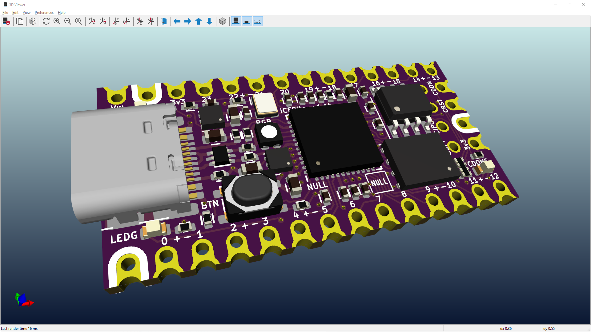
Key benefits:
- Mechanical fit checking
You can verify whether your board will fit inside an enclosure. This is crucial for products where space is tight. - Realistic rendering
With built-in ray tracing and adjustable lighting, KiCad can produce near-photorealistic images of your board. - Better understanding of the design
Seeing components in 3D helps you catch issues like:- Incorrect component orientation
- Clearance problems
- Connector placement mistakes
- Presentation-ready visuals
You can generate high-quality images to share your design with teammates, clients, or manufacturers.
👉 Example:
If you’re designing a wearable device, you can preview how connectors align with the casing and ensure buttons are accessible—before manufacturing anything.
What Makes KiCad Unique?
Beyond its individual tools, KiCad’s real strength lies in how everything works together.
1. Fully Integrated Workflow
You move smoothly from schematic → PCB layout → 3D visualization without switching tools or formats. Changes in one stage update across the entire project.
2. Open-Source Freedom
KiCad is completely open-source. This means:
- No licensing costs
- No feature restrictions
- A global community contributing improvements
3. Modern, Clean Interface
The latest updates bring a more polished and responsive experience. Tools are easier to find, actions feel faster, and the overall workflow is more intuitive.
4. Community and Libraries
A large user base contributes:
- Component libraries
- Tutorials
- Design examples
This makes learning and troubleshooting much easier.
5. Suitable for All Skill Levels
- Beginners can follow a straightforward path to their first PCB
- Advanced users can handle complex, high-density designs
A Simple Workflow Example
To better understand how everything fits together, here’s a typical workflow:
- Create a schematic
Place components like resistors, chips, and connectors, and connect them logically. - Run simulation and checks
Verify your design works and fix any errors flagged by the system. - Transfer to PCB layout
Arrange components on the board and route connections. - Validate the layout
Use design rule checks to ensure manufacturability. - Preview in 3D
Inspect the final board and confirm everything fits as expected. - Export for manufacturing
Generate files that can be sent directly to a PCB manufacturer.
Final Thoughts
KiCad represents a modern approach to electronic design: powerful, accessible, and open to everyone. It removes many of the traditional barriers—cost, complexity, and fragmentation—while still delivering professional-grade capabilities.
Whether you’re building a hobby project, developing a prototype, or working on a production-ready design, KiCad provides the tools to turn your ideas into reality with clarity and confidence.
License: Free and open-source
Website: https://www.kicad.org/